Chapter Technical Meeting
Tuesday, February 09, 2016
Holiday Inn Tewksbury
4 Highwood Dr, Tewksbury, MA 01876phone: (978)-640-9000
|
Ahmed Busnaina, William Lincoln Smith Professor, Distinguished University Professor and Director The NSF Nanoscale Science and Engineering Center for High-rate Nanomanufacturing Northeastern University 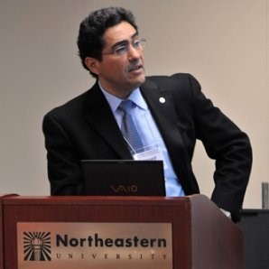
|
|
High-rate Nano and Microscale Printing of Electronics, Sensors, and Functional Materials Applications. |
| Printing offers an excellent approach to making structures and devices using nanomaterials, however, current electronics and 3D printing using inkjet technology, used for printing low-end electronics are slow and provide only micro-scale resolution. The NSF Center for High-rate Nanomanufacturing (CHN) has developed a new fully automated system that uses directed assembly based printing at the nanoscale to make products that fully take advantage of the superior properties of nanomaterials. The Nanoscale Offset Printing System (NanoOPS) can print metals, insulators and semiconductors (including III-V and II-VI), organic and inorganic materials into nanoscale structures and circuits (down to 20 nanometers). The fully automated robotic cluster tool system prints at the nanoscale to make products that take full advantage of the superior properties of nanomaterials. The NanoOPS has been used to print utilizing the following nanomaterials: nanoparticles, nanotubes, nanowires, 2D materials and polymers. The center has many applications where the technology has been demonstrated. The Center has shown a new way to print interconnects on any substrate as well as transistors and invertors using carbon nanotubes and 2D materials. The center has developed many sensors, among them a biosensor chip (0.02 mm) capable of detecting multiple biomarkers simultaneously (in vitro and in vivo) with a detection limit that’s 200 times lower than current technology. In addition, the center made a printed Band-Aid sensor that could read glucose, urea and lactate levels using sweat. An inexpensive micro chemical sensor with a low detection limit that’s less than 1 mm in size has also been developed. The Center also made many functional materials applications using nanoparticles and other nanomaterials to enhance plasmonic effects or reduce reflection on a variety of surfaces. |
|
SCHEDULE (times approximate): |
| 5:30 PM | Registration, Socializing, Networking & Cash Bar |
| 6:30 PM | Dinner |
| 7:30 PM | Technical Presentation |
Event Page